The Circuitry
THE CIRCUITRYYour one-stop source for all tech news
HOMETODAYNEWSFEEDEVENTS
BOOKMARKS
RSS
© 2026 The Circuitry
About UsSourcesContactCorrectionsPrivacy
  • Today
  • Feed
  • Events
  • Saved
Scroll for more
Verification
VERIFIEDConfidence: HIGH
Source identified
Claims cross-referenced
No discrepancies found
Fact-check summary

SemiAnalysis Oct 15 report and prior The Elec coverage confirm ASML's 27 bonding patent families signal D2W hybrid bonder development for advanced packaging.

Sourcing
1source

via DigiTimes Asia

DigiTimes Asia · track record
55Stories
100%Verified
1330d
All sources →
From The CircuitryWhy The Circuitry

Verified tech news, cross-checked.

Every story is checked against independent sources before it posts — no rumors dressed up as fact.

How we verify →
Home/Tech/ASML Patents Signal Hybrid Bonder for Advanced Packaging
VERIFIEDBy Xavier Rivera·Thursday, October 15, 2026 at 9:06 PM EDT·1 min read

ASML Patents Signal Hybrid Bonder for Advanced Packaging

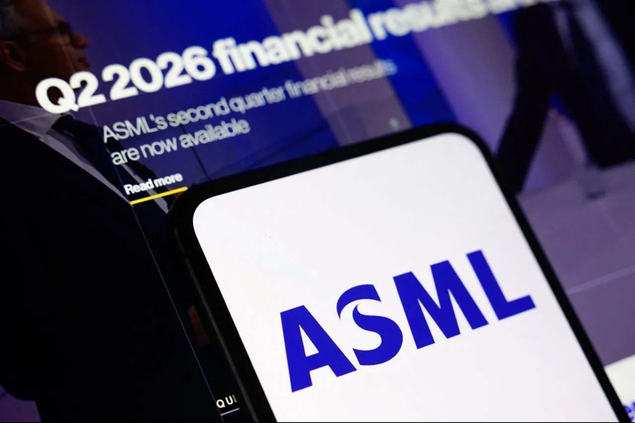
Patent filings analyzed by SemiAnalysis show ASML developing a die-to-wafer hybrid bonder for advanced packaging. The move positions the lithography leader against Besi and other suppliers as chipmakers seek growth beyond transistor scaling.
Source:DigiTimes Asia
Post
ASML Patents Signal Hybrid Bonder for Advanced Packaging
From The CircuitryWhy The Circuitry

Verified tech news, cross-checked.

Every story is checked against independent sources before it posts — no rumors dressed up as fact.

How we verify →
TL;DRAI · 60 sec read

ASML filed patents for a die-to-wafer hybrid bonder, marking its second push into advanced packaging equipment. The move comes as shrinking transistors grows costlier, prompting chip toolmakers to target packaging for growth. SemiAnalysis reviewed the filings, showing ASML will compete with Besi and other front-end suppliers.

ASML is preparing a move into advanced packaging equipment through new patent filings for a die-to-wafer hybrid bonder.
Advanced packaging draws equipment makers as transistor scaling grows costlier.
Advanced packaging draws equipment makers as transistor scaling grows costlier. The shift occurs because shrinking transistors has become harder and more expensive. Chip toolmakers now target packaging as their next area of growth.
From The CircuitryThe Feed — live briefs across tech, all day.See what’s happening →
Patent analysis points to ASML's hybrid bonder development. Research firm SemiAnalysis examined the filings from the Dutch lithography company. The work indicates ASML is building a die-to-wafer hybrid bonder as its second entry into the packaging space.
ASML would compete with Besi and other front-end suppliers.
ASML would compete with Besi and other front-end suppliers. Besi currently leads in this segment. A growing group of front-end rivals is also pursuing the same market opportunity.
From The CircuitryWhy The Circuitry

Verified tech news, cross-checked.

Every story is checked against independent sources before it posts — no rumors dressed up as fact.

How we verify →
The filings mark ASML's renewed focus on packaging tools. The company previously explored the area and now appears to be expanding its efforts based on the analyzed patents.
Why this mattersAI · ~100 words

Tap a lens to see what this story means for you.

Morning Brief

Liked this? The Brief brings you the whole day in tech, verified, every morning.

Two minutes, free forever. What's in The Brief →

Reader-supported
DonateBuy me a coffee →Follow@thecircuitry_ →Follow@thecircuitry.to →
HELP US IMPROVE
From The Circuitry

See what’s happening right now

The Feed runs all day — short, verified briefs the moment they break.

Open the Feed →
From The Circuitry

Follow @thecircuitry_

Every story we publish, as it happens. No noise between.

Follow on X ↗On Bluesky ↗

Reader-supported

The Circuitry is a passion project I've always wanted to build, and I love the work behind it.

Running it costs real money. APIs, hosting, time. To keep improving the site and growing this into something useful for everyone, those costs have to be covered.

Any contribution is appreciated. If not, no pressure. Thanks for reading.

Buy me a coffee
semiconductorsASMLpackaging
More fromDigiTimes Asia
  • DigiTimes: ByteDance in advanced talks with MediaTek for custom data center chips

    Tech · 1h
  • GlobalFoundries to run up to two Japan-funded New York fabs in $21B deal

    Tech · 1d
  • DigiTimes: Moonshot AI seeks to resolve US$700 million dispute before Hong Kong IPO

    Tech · 3d
More inTech
  • Tesla Unveils Its Next-Gen Roadster: Everything Announced

    Tech · 15m
  • Stuntman: Hollywood Shows Knight Rider K.I.T.T. Gameplay

    Tech · 1h
  • Microsoft SharePoint Server Subscription Edition hit by CVE-2026-108452

    Tech · 3h
SupportThe Work

The Circuitry is reader-supported. If you find the daily brief useful, you can buy me a coffee to keep it going.

Buy a coffee →
From The CircuitryWhy The Circuitry

Verified tech news, cross-checked.

Every story is checked against independent sources before it posts — no rumors dressed up as fact.

How we verify →

MORE IN THIS BEAT

All Tech →
  • Tech·Oct 8

    GlobalFoundries signs $2B TSMC deal for US silicon interposers

    GlobalFoundries signed a multi-year US$2 billion agreement with TSMC on October 8, 2026 to manufacture silicon interposers at its Malta, New York fab. The deal creates the first US-based source of silicon interposers for TSMC's CoWoS advanced packaging ecosystem.

  • Tech·Jul 15

    Intel Ships First High-NA EUV Logic Product for Panther Lake

    ASML confirmed on July 15 that Intel Foundry shipped the first high-volume logic product made with High-NA EUV lithography for Panther Lake. The milestone advances commercial readiness of the technology while ASML prepares TSMC and Samsung for wider adoption.

  • Tech·Oct 15

    DigiTimes: ByteDance in advanced talks with MediaTek for custom data center chips

    DigiTimes: ByteDance is in advanced talks with MediaTek to buy custom data center chips, and an agreement could come soon, according to people familiar with the matter. Bloomberg first reported the talks, saying a deal would help MediaTek compete with Qualcomm and Broadcom in data centers.

  • Tech·Oct 14

    GlobalFoundries to run up to two Japan-funded New York fabs in $21B deal

    GlobalFoundries will operate up to two new chip fabs at its Malta, New York, site under a U.S.-Japan initiative providing up to $21 billion, with Japan supplying the money. The first fab, about $10 billion, is due online in 2029; a second, about $10 billion more, is still subject to approval.

  • Tech·Oct 6

    Marvell lifts 2028 revenue target to approximately $20B on AI connectivity

    Marvell Technology raised its fiscal 2028 revenue outlook to approximately $20 billion and set a fiscal 2031 target of $70-90 billion. The increases reflect expected growth in AI networking and optical connectivity demand.